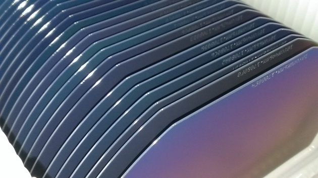
A wafer refers to a piece of semiconductor material, like silicon crystal, that can be used to fabricate integrated circuits as well as micro devices. In this case, the wafer will act as a substrate for microelectronic devices that sandwich the wafer and passes through various micro fabrication processes like photo lithographic patterning, etching, ion implantation and deposition of several materials.
Silicon makes up the second largest Earth component and is the 7th most used element universally. Most semiconductors are made of it with a wide range of applications in the technology sector. It thus makes sense to see how popular silicon wafer is.
The cost
The pricing of silicon wafer is based on diameter with the least price is about US $1 per square inch of the 125mm diameter. There is also a medium price which is US $2 per square inch of the 200mm diameter. For the 300mm diameter silicon wafer, the cost is about US $3 per square inch. This gives a maximum of US $400.
Here is a quick summary for the cost of silicon wafer
- 125mm diameter — US $1 per square inch
- 200mm diameter — US $2 per square inch
- 300mm diameter — US $3 per square inch
One factor to note is that anytime a new silicon wafer is introduced, the cost of silicon wafer will be at peak. But this price drops with time as the technology matures.
Uses of silicon wafer
So what are some of the applications of the silicon wafer?
The modern day world has got so many uses and applications for these, making it a challenge to categorize the uses. It also proves difficult to just pick a few uses and base on them.
The cast of silicon wafer may be costly but these elements are highly useful. Electronic devices chips and microchips are manufactured using silicon wafers. Due to the features that they possess, they are used in the making of integrated circuits (lCs). The 1Cs are then applied in various electronic gadgets.
As much as you may want to link the silicon wafers with some technical devices that you probably thought you can never get hold of, they are always around us! Are you aware that they are in mobile phones, computers as well as the smart phone you probably are using now? And what about the tire pressure sensor system? Well, it is there as well!
Many companies have also learnt the importance of using silicon wafers to test their products. This use entails creation of prototype or product for testing. It is possible that the silicon will get damaged during the process. Of course in the past this would turn out problematic as new silicon had to be bought. But advances in technology have brought with it a set of advantages. Today, that is no longer a necessity.
After using a wafer, companies are free to send back the wafer through a reclaim process to the service provider for recycling. This helps to reduce the cost of silicon wafer to a price that is manageable. On the other hand, companies get to save for their next big project.
