Why is silicon used for the fabrication of semiconductor devices?

silicon

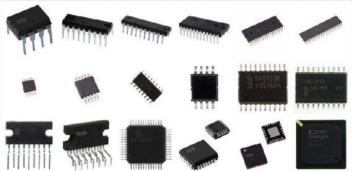
Silicon (Si) is the most extensively utilized component in semiconductor gadgets. Its mix of cheap raw material price, reasonably easy processing, and also a useful temperature level make it currently the best compromise amongst the different competing components.


The main reasons are the following: –


  1. Silicon is cheaper because of 8th most popular element by mass as well as plenty offered on the surface of the our planet.


  1. Silicon can conveniently able to react with oxygen and also generates SiO2 that is utilized as a best insulator in semiconductor industry as a dielectric as well as in IC manufacture procedures like diffusion, Ion implantation.


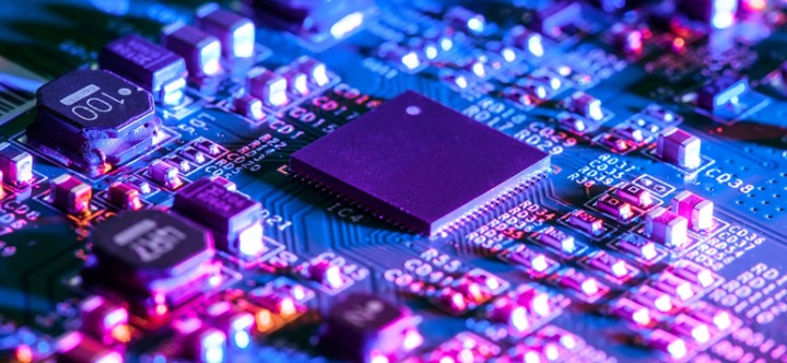
  1. While effective transistors are preferable, the actual target is integration, placing billions of transistors on the same chip. A stable oxide and effective substratum isolation were secrets to silicon’s success.


  1. Silicon has a far better temperature level , low leakage, and is less expensive, one point which guaranteed its development.


  1. Since of availaibility of free electrons in its valence shell, Silicon has greater conductivity.


  1. Silicon can be simply oxidized to develop thin layer of SiO2 (needed below the gate) and thick oxide utilized else where to separate parts or wells from each other. All it takes is completely dry N2, H20 as well as temperature level regulated oven.


  1. Silicon has high band gap. So much less leak current. High temperature level stability.


  1. The thermal dioxide of Silicon can be much more pure and also versatile to development directly on device surface, which is can be more thin, much more stable, having small internal flaws density.

How Integrated Circuits Are Made

Integrated Circuits

You don’t have to find out how integrated circuits (IC) are manufactured to use them in your electronic devices, yet the process is very interesting The procedure is complex and varies depending upon the type of chip being manufactured. However, the adhering to process is common:

  1. A large, cylindrical piece of silicon crystal is cut right into thin wafers about one-hundredth of an inch thick. Each of these wafers will be utilized to create several hundred or many thousand finished integrated circuits.
  2. A special photoresist solution is deposited on top of the wafer.
  3. A mask is applied to over the photoresist. The mask is an image of the real circuit, with some regions transparent to allow light through and others opaque to block the light.
  4. The wafer is exposed to extreme ultraviolet light. The ultraviolet light engraves the wafer under the transparent portions of the mask but leaves the regions under the nontransparent parts of the mask untouched.
  5. The mask is gotten rid of and also any type of remaining photoresist is cleaned off.
  6. The wafer is after that exposed to a doping material. This makes p-type and n-type regions in the etched regions of the wafer.
  7. The process is repeated for each and every layer till every one of the layers have been created. Of course, this presumes that the circuit design requires multiple layers stacked on top of each other.
  8. The particular integrated circuits are then sliced apart and installed in their final packaging.


Right here are a few other tidbits worth knowing about how integrated circuits are made:

– As you have probably seen on Intel commercials, the manufacturing procedure for integrated circuits is done in a tidy place, where employees use unique suits as well as masks. This is essential because at the range of the integrated circuits, even the smallest speck of dust is enormous.

– Each integrated circuit undergoes a variety of complicated quality examinations after the circuit is finalized. The manufacturing process is by no means perfect, many are thrown out.

To know more about wafers visit www.waferpro.com

Several Types of Semiconductor Products

Semiconductor Products

In order to be suitable as a semiconductor product, a material is needed to have electric conductivity which lies in between that of an insulator that conducts extremely minimal amount of electrical energy, and conductors which allows electrical power to flow smooth and easily. Semiconductors created from amorphous solids and liquids also exist.

A semiconducting product can raise their conductivity by subjecting it to magnetic fields, electricity energy or other stimuli which raises the energy level of the product’s electrons. This allows electrical energy to flow through the semiconductor.

By controling the semiconductor’s conductivity, it can also be utilized as a switch. Semiconductors are also utilized for lots of other reasons like solar energy generation and light detecting sensors. This is due to the fact that they can generate a circulation of electricity current when appropriate energized by incoming photons of light.

Semiconductors also include little amounts of dopants utilized to modify their conductive properties appropriately to match their functions much better. Gallium nitride and gallium arsenide doped with metals have both semiconducting and ferromagenetic properties like manganese.

The other most generally utilized semiconductor product is silicon. Several semiconductors that are created of silicon often have a normal crystalline structure in that their atoms are organized. Amorphous silicon semiconductors have weaker efficiencies as compared to crystalline silicon.

Another gallium compound which is utilized for semiconductors is also the gallium nitride (GaN). It is also utilized in light producing diodes (LEDs), military radars and high frequency laser diodes. It can also be integrated with numerous other semiconductor products like indium nitride (InD) to generate a mixture.

The next most basic semiconductor product apart from Silicon is also the compound gallium arsenide (GaAs). It is also more expensive and more very difficult to process at the same time. In addition, it also results in greater power usage.

Basic semiconductor products also consist of gallium arsenide, gallium nitride and silicon though others might also exist. In addition, to these main products, semiconductors are commonly in little amount of other materials. They are referred to as dopants.

To buy semiconductor products visit www.waferpro.com

Semiconductor and Silicon Wafer

integrated circuits (ICs)

What is a semiconductor?

A Semiconductor can be represented as a material which has the attributes and capability to conduct a little amount of electric current in a regulated way. The electric energy of a semiconductor can be managed over a broad variety, either permanently or dynamically.


Material Applied to Produce Semiconductors

Silicon is the most commonly utilized semiconductor material. Several other materials utilized in producing semiconductor are germanium, gallium arsenide, and silicon carbide.


What is a Silicon Wafer?

A wafer is a slice of semiconductor material, typically silicon crystal. These wafers are utilized to make integrated circuits (ICs) and other microdevices. Silicon wafers are readily available in a variance of sizes varying from 25.4 mm (1 inch) to 300 mm (11.8 inches).

What are Semiconductors?

Semiconductors are elements that have a conductivity between conductors (usually metals) and also non-conductors or even insulators (just like ceramics). Semiconductors is generally clean components, like silicon or germanium, as well as elements just as gallium arsenide and even cadmium selenide. In a procedure named doping, small amounts of impurities are included with clean semiconductors making huge improvements in the conductivity of the substance.

Semiconductors

Because of their character in the manufacture of electrical equipments, semiconductors are a part of our everyday life. Just imagine living without electrical equipments. Generally, there will be no radios, no TV’s, no laptops or computers, no computer games, and poor healthcare diagnostic machines. However, several electrical equipments can be made with vacuum tube technique, the improvements in semiconductor devices in past fifty years are making electrical equipments smaller sized, much faster, and efficient. Consider for a minute of the experiences you will have with electrical equipments. Several of the following ever found or even utilized in the previous 24 hrs? All possesses essential parts which have been produced with electrical products.

Improvements in the field of electronic devices will remain to help our everyday life. Researching electrical products will help you understand and take part in the aspects of communication, laptops or computers, medicine, the basic sciences as well as technology. All these aspects use electronic devices commonly.

Visit WaferPro to buy semiconductor products at a cheap price.

What A Wafer Supplier Can Offer You

It doesn’t matter why you’d like to purchase wafers, searching for a superior and trusted wafer seller is really important. Still, selecting a superior seller isn’t an easy task. There are many tips that you’ve to decide upon for selecting a superior one. It’s advisable to observe some basics for choosing the right one. Generally, there are lots of aspects which come into play when selecting a seller. Firstly, it’s very important to ensure that the trader you have chosen provides the best quality products to the users. Secondly, the firm ought to be have an understanding of your requirements and provide the best suited good quality products.

Silicon Wafer

If a supplier has a good popularity in the market, you’ll have a guarantee on the products they give. When choosing a seller plays an essential factor in the entire aspects of the project, it’s very important to find the perfect one with caution. In addition to this, they need to provide you suggestions on the project that you’re dealing with and provide the appropriate wafers suited to the project. Even if there are many options for selecting a seller, searching on the internet is regarded as the most effective. While you’re browsing online for wafer dealers, you’ll discover many possibilities in front of you. That will let you to choose the best one, that agrees with your requirements and expense plan.

Looking at several wafer suppliers using internet is usually a wonderful way to select the right for your needs. However, while you’re comparing it’s very important to maintain several important things in your mind for example the experience of the firm, popularity, costs, offers etc. It’s also wise to be sure that the products supplied by the firm are reasonably priced and durable. In case, if you aren’t able to decide on a good Wafer Seller without any help, taking the help of an expert will be the smartest choice in your case. There are lots of experts using internet, who will assist you in selecting the right seller for your needs. This ensures you are selecting a trader, who can supply you the best quality wafer products for the money you invest.

Semiconductor Types And Uses

Semiconductors are elements which use amazing influence on human everyday life. In each and every device that individuals use, Semiconductors can be found in all places – in microprocessor chips or transistors or any imperative device that we easily use in our everyday activities. In the Semiconductor manufacturing business there are many big competitors. It has become a multi-billion dollar business right now. Inside our day-to-day everyday life everyone use lot of such devices or items that have Semiconductors as their main part – from microwave to microprocessor chips to transistors to pcs. In pcs which are life to most of us have those Semiconductors at their heart. Almost all the Semiconductors are made from silicon, which is why silicon is heart of any electronic devices.

Semiconductor

 Among all Semiconductor manufacturing gadgets, diode is a most effective one. This is the important part of all Semiconductors which are usually utilized in the fabless engineering sector or other business. The most usually specially designed substances like ASIC types, integrated circuits and microprocessor manufacturing, all over silicon is a major component. An additional necessary element is germanium that’s especially utilized in transistors and various electronics. It’s utilized in several industries such as fiber optics and infrared optics. Also, it is found in polarization catalysts, solar cell uses etc. A further favored Semiconductor is Gallium arsenide. It’s actually an III/ V Semiconductor and it is widely utilized in the manufacturing of gadgets like microwave frequency integrated circuits, infrared light-emitting diodes, monolithic microwave integrated circuits, solar cells, laser diodes, and inside manufacturing of optical windows.

 Whereas developing the silicon Semiconductor materials, manufacturing is a major process. It requires several significant techniques. Crystal preparation is the initial step that starts the method. In this process a single crystal of silicon is produced into a solid cylindrical form. After that silicon wafer preparation is done when solid cylinder of silicon is cut with a diamond saw blade consistently. After that thin film generation is done where physical or electrical isolation between two adjoining layers comes or wafer is prepared for doping along with lithography stages. In this case Lithography is a process at which designs on substances are customized. Then the major action is completed where high precision flat metal substances are produced, that’s known as chemical milling. Moreover, doping is completed at which we add pollutants into a very pure Semiconductor. The process is designed to modulate the electrical properties of a Semiconductor. Lastly, metallization is completed where product is treated and merged with a metal. This finishes the procedure.

Cost of silicon wafer and common semiconductor applications

A wafer refers to a piece of semiconductor material, like silicon crystal, that can be used to fabricate integrated circuits as well as micro devices. In this case, the wafer will act as a substrate for microelectronic devices that sandwich the wafer and passes through various micro fabrication processes like photo lithographic patterning, etching, ion implantation and deposition of several materials.

Silicon wafers
Silicon wafers

Silicon makes up the second largest Earth component and is the 7th most used element universally. Most semiconductors are made of it with a wide range of applications in the technology sector. It thus makes sense to see how popular silicon wafer is.

The cost

The pricing of silicon wafer is based on diameter with the least price is about US $1 per square inch of the 125mm diameter. There is also a medium price which is US $2 per square inch of the 200mm diameter. For the 300mm diameter silicon wafer, the cost is about US $3 per square inch. This gives a maximum of US $400.

Here is a quick summary for the cost of silicon wafer

  • 125mm diameter — US $1 per square inch
  • 200mm diameter — US $2 per square inch
  • 300mm diameter — US $3 per square inch

One factor to note is that anytime a new silicon wafer is introduced, the cost of silicon wafer will be at peak. But this price drops with time as the technology matures.

Uses of silicon wafer

So what are some of the applications of the silicon wafer?

The modern day world has got so many uses and applications for these, making it a challenge to categorize the uses. It also proves difficult to just pick a few uses and base on them.

The cast of silicon wafer may be costly but these elements are highly useful. Electronic devices chips and microchips are manufactured using silicon wafers. Due to the features that they possess, they are used in the making of integrated circuits (lCs). The 1Cs are then applied in various electronic gadgets.

As much as you may want to link the silicon wafers with some technical devices that you probably thought you can never get hold of, they are always around us! Are you aware that they are in mobile phones, computers as well as the smart phone you probably are using now? And what about the tire pressure sensor system? Well, it is there as well!

Many companies have also learnt the importance of using silicon wafers to test their products. This use entails creation of prototype or product for testing. It is possible that the silicon will get damaged during the process. Of course in the past this would turn out problematic as new silicon had to be bought. But advances in technology have brought with it a set of advantages. Today, that is no longer a necessity.

After using a wafer, companies are free to send back the wafer through a reclaim process to the service provider for recycling. This helps to reduce the cost of silicon wafer to a price that is manageable. On the other hand, companies get to save for their next big project.